

GMK Semiconductor operates within the broader GMK World ecosystem, a diversified industrial group with presence across:
Technology and manufacturing
Power, aviation, logistics, and cold storage
Agriculture, seafood, and life sciences
Media, broadcasting, and global investments
The company is founded and led by the Joshi Brothers, first-generation entrepreneurs driving an integrated philosophy of economic development, sustainability, and global security.
GMK Semiconductors
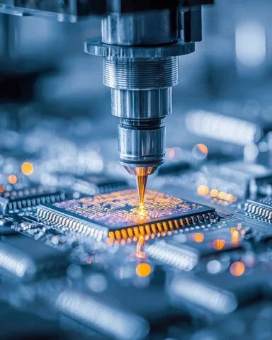
Advanced Semiconductor Manufacturing, Foundry & Technology Platforms
Our Expertise
-
DesGMK Group Context & Leadership
GMK Semiconductor operates within the broader GMK World ecosystem, a diversified industrial group with presence across:
Technology and manufacturing
Power, aviation, logistics, and cold storage
Agriculture, seafood, and life sciences
Media, broadcasting, and global investments
The company is founded and led by the Joshi Brothers, first-generation entrepreneurs driving an integrated philosophy of economic development, sustainability, and global security.
-
DescGMK Semiconductor is anchored in strong global and national drivers:
Rapid growth in global semiconductor demand driven by AI, EVs, IoT, 5G, and cloud computing
Increasing geopolitical realignment and supply-chain de-risking
India’s rising electronics consumption and import dependence
National imperatives for sourcing stability, security, and self-reliance
The initiative supports India’s ambition to become a semiconductor manufacturing nation, complementing its existing strength in chip design.ription text goes here
-
GMK Semiconductor specialises in logic and specialty IC manufacturing, with capabilities including:
Embedded high voltage technologies
Embedded non-volatile memory
RF-SOI
BCD processes
The company’s fabrication strategy focuses on mature and specialty nodes, balancing scalability, cost efficiency, and broad industry applicability.
-
Phase I
Investment of approximately ₹10,000 crore
Establishment of India’s first elite commercial semiconductor foundry
300mm Silicon Photonics and 200mm GaN on Silicon
Capacity of ~20,000 wafers per month
Technology nodes ranging from 28nm to 180nm
Located within a high-tech industrial park to enable a self-sustaining semiconductor ecosystem
Phase II
Expansion to 40,000 wafers per month
Continued focus on 300mm manufacturing
Strengthening India’s position in mature-node and specialty chip production
This phased approach prioritises capital discipline, operational efficiency, and long-term demand alignment.
-
GMK Semiconductor adopts an India-HQ–centric model, differentiating itself from satellite fab structures by:
Retaining core technology, expertise, and decision-making within India
Onboarding 30+ global foundry experts
Supporting domestic fabless companies and allied semiconductor industries
Reducing long-term dependency on foreign-controlled fabs
This model aims to build enduring national capability, not just manufacturing capacity.
-
DescGMK Semiconductor is anchored in strong global and national drivers:
Rapid growth in global semiconductor demand driven by AI, EVs, IoT, 5G, and cloud computing
Increasing geopolitical realignment and supply-chain de-risking
India’s rising electronics consumption and import dependence
National imperatives for sourcing stability, security, and self-reliance
The initiative supports India’s ambition to become a semiconductor manufacturing nation, complementing its existing strength in chip design.ription text goes here
-
Beyond foundry operations, GMK Semiconductor supports innovation across:
AI, IoT, and next-generation computing
Cloud-based server and edge infrastructure
Energy systems including PV modules and microgrids
Industrial intelligence, automation, and carbon management platforms
Healthcare and smart-device applications
The vertical is positioned as an enabler of cross-sector technological convergence.